A few weeks ago Elektra and I started Phase 2 of the Mesh Potato project. In Phase 2 we are working with Atcom to build the prototype Mesh Potato hardware. The first work package is hardware design.
Elektra is working on hardening the various ports of the Mesh Potato against environmental and accidental damage. For example making sure the power port is robust to reverse DC connection, and protecting the Antenna and Ethernet ports from static. She is also taking particular care to ensure that the power supply is as efficient as possible; saving a few watts really matters in solar powered applications.
I am working on the FXS interface hardware. The Atheros SoC chips have a lot of functionality, but unfortunately don’t have a Time Division Multiplexed (TDM) bus peripheral which is required to connect to the FXS chipset. The current plan is to make a RS232 serial to TDM adaptor, using some programmable logic. Speech samples will flow through the Atheros SoC RS232 serial port to and from the TDM bus.
The software side of the FXS interface involves modifying the serial driver (8250.c in the kernel), to store speech samples in buffers that are then uploaded to user mode for Asterisk. It is important that the interrupt service routine is really fast, so I am bypassing much of the standard serial code and writing a custom ISR.
Over the last few weeks I have written the modified driver and tested it using RS232 signals from a PC. This week I have been designing and testing the hardware side of the interface. This involves writing a bunch of Verilog code, then testing it using a PC based simulator. I am using the (open source) Icarus and GTKwave programs to simulate and visualise the waveforms. It’s much easier to test and debug all this complex logic in simulation form before firing up any hardware.
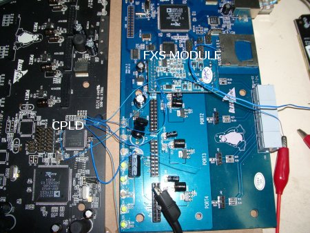
Over the last few days I have been testing all this logic using a prototype jig:

Two IP04s are used. IP04s happen to have a Xilinx CPLD chip on board that is suitable for running the FXS Interface logic. So on the LH IP04 I reprogrammed the CPLD with the FXS Interface logic. The right hand IP04 in the picture above is used as “life support” for a FXS module. The FXS module runs as per normal on the IP04 but we tap off the various TDM bus signals we need to drive the CPLD on the IP04 on the left. So to test I can speak into a phone connected to the IP04 and the CPLD does it’s thing with the signals, converting them to and from RS232 serial.
So far I have tested both the receive and transmit side of the FXS Interface by connecting the serial signals to a PC. I managed to sample my own voice by capturing the RS232 bytes to a file and playing it back on my PC’s sound card. So far so good.
Today I have started connecting the FXS Interface to a Nanostation 2. My first tests crashed the Nanonstation! I guess due to something I changed on the serial driver. So time for some debugging……
Links
Verilog Tutorial
FXS Interface Verilog source and test benches
README documenting FXS Interface design
FXS Interface timing diagrams in gschem format